

| หากต้องการใบเสนอราคา / ใบแจ้งหนี้ ติดต่อได้ทาง LINE Official: @mikroelec |
 |
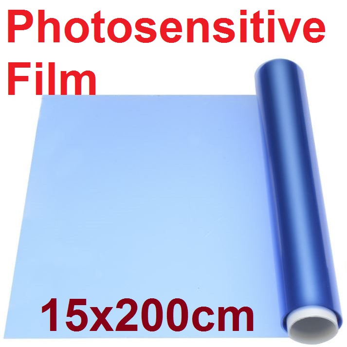
dry film 15x200cm. Portable Photosensitive Film for Circuit Photoresist Plate Plating Hole Covering Electroplating PCB Board


| รหัสสินค้า | SKU-01845 |
| หมวดหมู่ | อุปกรณ์ DIY กัดปริ๊น ลายวงจร |
| ราคา | 100.00 บาท |
| สถานะสินค้า | พร้อมส่ง |
| ลงสินค้า | 20 ม.ค. 2565 |
| อัพเดทล่าสุด | 9 พ.ค. 2568 |
| จำนวน | ชิ้น |
หยิบลงตะกร้า

รายละเอียดสินค้า
Photosensitive film is also called dry film . It is used to make PCB circuit boards. When it is pasted on the PCB circuit board , it becomes a photosensitive circuit board (because the photosensitive circuit board is more expensive ). It is simple to use it as a PCB circuit board. Convenience , easy to make, etc.
feature:
-Take pictures, also known as film, to make the PCB board, stick it on the PCB to become a Sensitive Circuit Board.
- Suitable for plating, hole covering, and carving processes.
- Excellent ability to cover holes
- high resolution
- Excellent adhesion to almost all surfaces
- Image Clarity after exposure
-Front-panel clean after development
Size: 15x200cm/5.91''x78.74''
30X100ซม./11.81 "x 39.37"
Color: As the picture shown
How to use:
1. Grinding the copper clad laminate, this is simple, just use the finest water-grinding sandpaper to polish it clean. (This step is not necessary, as long as there is no oil stain on the board, this step can be omitted)
2. Peel off the film, the photosensitive film is sandwiched between two layers of film, tear off one side first and tear it off with the help of transparent tape, Just a few more tries.
3. Then stick the film, clean the copper plate a little, stick it flat, try not to have air bubbles
4. Use the plastic machine after sticking the film, do not need to be too hot, and fix it from about 100 degrees.
5. For the printed circuit board film, it is recommended to use the film, which can achieve the highest fineness. If the precision is not required to be printed with sulfuric acid paper. (The picture below is the high-precision inkjet film)
6. Put the printed circuit diagram on the photosensitive plate, (note: the dry film is negative, so it must be printed in reverse, which is positive with the photosensitive plate we usually use Conversely) use an ordinary energy-saving lamp for about 10 minutes, if you have an exposure machine for 1 minute, I have not tried it under the sun, it should be about 30-60 seconds, the exposure process is obvious, because the photosensitive film will change color during exposure, from light color to dark blue . You will easily see your circuit diagram appear on the board.
7. For development, tear off the protective film on the panel and put it in the developer (the developer is 1:100, 10 grams of water in total 1L). When developing, you can use a cotton stick to wipe the test board with a little force.
8. Etching, needless to say (ferric chloride, environmentally friendly etchant, hydrochloric acid + hydrogen peroxide, etc.) It is recommended to use our environmentally friendly etching, which is fast, clean and odorless.
9. After etching the copper clad laminate, remove the film, mix the release agent with water at 1:60 or 70, and soak the board for a few minutes.
engrave
Dry the film can get the most of the acid etching solution, the PH value can be waterproof most alkaline etching solution between PH8.0~8.5.
Hole cover
1.5 MIL, fully dry film, 0.25 in. hole.
plated
Dry film is available in general use with plating bath, no wrinkle, no color.
Package included:
1 roll of light film
วิธีการชำระเงิน
ชำระเงินผ่านธนาคาร
ชำระเงินด้วยการ Scan QR


ไมโครอิเล็กทรอนิกส์
098-xxxxxx-9
Accept All Banks | รับเงินได้จากทุกธนาคาร
นโยบายการเปลี่ยนหรือคืนสินค้า
หากสินค้าชำรุดหรือใช้งานไม่ได้ สามารถขอเปลี่ยนสินค้าได้ภายใน 7 วัน
หมายเหตุ
ต้องไม่เสียหายอันเกิดจากใช้งานผิดพลาด ใช้ผิดวิธี ต่อไฟผิดขั้ว จ่ายไฟเกินกำหนด หรืออื่นๆที่ตรวจสอบแล้วไม่ได้เกิดจากความผิดพลาดจากการผลิตสินค้า
หมายเหตุ
ต้องไม่เสียหายอันเกิดจากใช้งานผิดพลาด ใช้ผิดวิธี ต่อไฟผิดขั้ว จ่ายไฟเกินกำหนด หรืออื่นๆที่ตรวจสอบแล้วไม่ได้เกิดจากความผิดพลาดจากการผลิตสินค้า

Member
▲
▼
รายการสั่งซื้อของฉัน
รายการสั่งซื้อของฉัน
ข้อมูลร้านค้านี้

MikroElectronic
จำหน่ายอุปกรณ์อิเล็กทรอนิกส์ โมดูล เครื่องมือ และอุปกรณ์ต่างๆ arduino อาดูโน อะไหล่เครื่องใช้ไฟฟ้า อะไหล่อิเล็กทรอนิกส์ รับออกแบบวงจร เขียนโปรแกรมด้วยอาดูโน รับทำโครงงาน นักเรียนนักศึกษา ให้คำปรึกษาแก้ปัญหาโครงงาน ออกแบบและสร้างงานต้นแบบ ร้านตั้งอยู่ ซอยร่วมสุข ปทุมธานี สถานที่ใกล้เคียง ดอนเมือง สรงประภา ศรีสมาน นนทบุรี แจ้งวัฒนะ
เบอร์โทร : 0984829329
อีเมล : mikroelec@gmail.com
อีเมล : mikroelec@gmail.com
ส่งข้อความติดต่อร้าน
เกี่ยวกับร้านค้านี้
ค้นหาสินค้าในร้านนี้
ค้นหาสินค้า
สินค้าที่ดูล่าสุด
บันทึกเป็นร้านโปรด
Join เป็นสมาชิกร้าน
แชร์หน้านี้
แชร์หน้านี้
↑
TOP เลื่อนขึ้นบนสุด
TOP เลื่อนขึ้นบนสุด
สินค้าในตะกร้า ({{total_num}} รายการ)

ขออภัย ขณะนี้ยังไม่มีสินค้าในตะกร้า
ราคาสินค้าทั้งหมด
฿ {{price_format(total_price)}}
- ฿ {{price_format(discount.price)}}
ราคาสินค้าทั้งหมด
{{total_quantity}} ชิ้น
฿ {{price_format(after_product_price)}}
ราคาไม่รวมค่าจัดส่ง
รวมภาษีมูลค่าเพิ่มแล้ว
➜ เลือกซื้อสินค้าเพิ่ม